

Integrated Engineering Architectures and Operational Probe Card Market Solution Deployments

A complete, modern Probe Card Market Solution represents an intricate electro-mechanical system engineered to deliver high-frequency electrical signals between automated test equipment (ATE) and microscopic wafer pads. The solution architecture consists of several primary sub-assemblies: the printed circuit board (PCB), the multi-layer organic (MLO) or multi-layer ceramic (MLC) space transformer, the probe head containing thousands of micro-contacts, and stiffener hardware to maintain mechanical planarity. Each component must be precisely manufactured and assembled to ensure sub-micron contact accuracy and continuous electrical performance across variable temperature test environments.
The printed circuit board functions as the primary electrical routing interface, connecting high-density tester channels to the space transformer. As signal frequencies rise above tens of gigahertz in AI and 5G test applications, designing low-loss PCB routing channels with optimized impedance matching becomes critical. The space transformer sits between the PCB and the probe head, translating wider electrical trace pitches from the circuit board down to the tight micro-pitches of the probe array. Advanced multi-layer ceramic substrates are favored in high-density solutions due to their mechanical rigidity, thermal stability, and ability to route tens of thousands of independent signal paths without electrical crosstalk.
At the physical interface with the semiconductor wafer, the probe head houses the micro-contact tips. In modern MEMS solutions, these contacts are micro-fabricated using photolithographic techniques, producing spring-like structures that flex upon touchdown. This controlled deflection penetrates surface oxide layers on wafer pads, establishing stable, low-resistance electrical connections while applying minimal mechanical force. Proper tip geometry design and material selection prevent physical damage or metal splatter on delicate pad surfaces, ensuring that tested wafers remain suitable for subsequent wire bonding or flip-chip bump assembly.
Finally, modern probe card solutions incorporate diagnostic monitoring features and modular maintenance capabilities. Modular probe heads allow test operators to replace damaged or worn probe clusters in the field, reducing repair lead times and maintaining operational availability. Integrated temperature sensors and stress gauges continuously track environmental conditions during wafer probing, alerting test engineers to thermal gradients or mechanical misalignments. By combining high-density signal routing, precision micro-mechanics, and automated diagnostic capabilities, modern probe card solutions deliver the performance required for advanced wafer verification.
Top Trending Reports :
South Korea Kids Smartwatch Market
India Kvm Market
Categorias
Leia mais
The reallocation of global premium volumes indicates that a significant percentage of Internet of Things IoT Insurance Share is moving rapidly toward organizations that prioritize end-to-end digital transformation. Historically, established insurance giants dominated the industry through vast agent networks and deep financial reserves, showing little urgency to adopt real-time sensor...

In late 2025, The Company announced a landmark agreement to invest 1 billion in and license 200 characters for use in the AI video generation tool and app. brings more than two decades of experience across luxury and premium brands, including. To attract fashion users, launched its collage functionality in late, allowing users to pull together outfits from different pins and mood boards, which...

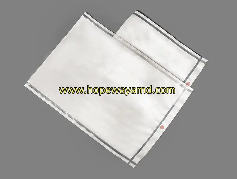
In healthcare packaging, every material choice can influence how a product is prepared, processed, stored, and handled. The Tyvek Breathing Bag from Hopeway AMD presents a breathable packaging concept designed for applications where controlled permeability and protective structure need to work together. By combining practical bag construction with material characteristics suited to...
Deploying agile, cloud-native transaction processing modules offers a highly dependable path forward via the Core Banking Solution Market Solution. By breaking down rigid, old system code into separate functional blocks, these modern systems eliminate processing bottlenecks across multichannel retail networks. This flexible software setup ensures that sudden spikes in mobile application...

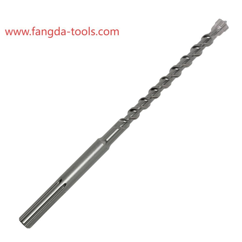
In construction and renovation work, choosing the right tools directly affects both efficiency and final results. The Fangda Hammer Drill Bit is widely used for penetrating dense surfaces such as concrete, brick, and stone. With a focus on durability and practical functionality, fangda-tools provides solutions tailored to meet the expectations of users who require steady performance in...